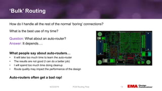
Your Route to Design Success PCB Routing Tips from the Pros Circuit Diagram Complex PCB routing requires rules and constraints for success. As PCB designers, setting up rules and PCB design constraints for routing a printed circuit board is a critical part of our job. It can take time and involve research and manual input, but setting up these constraints and routing your board according to the rules can save your
PCB routing is a complex yet essential aspect of circuit design that directly impacts the performance, reliability, and functionality of electronic devices. Mastering PCB routing techniques, from circuit design and trace optimization to high-speed routing and signal integrity, is crucial for creating efficient and reliable PCBs.

Mastering PCB Routing: Techniques for Optimal Circuit Design and ... Circuit Diagram
AI-driven routing improves signal integrity and power distribution while adhering to strict DFM and DFA constraints. Allegro X AI automates component placement, power plane creation, and critical net routing. Generative AI for PCB design is transforming the way we design, offering new efficiency and optimization for workflows.
PCB routing is an essential step in the design process that significantly impacts the performance and reliability of electronic devices. By following best practices such as proper trace width selection, effective ground and power plane usage, and controlled impedance routing, designers can ensure optimized signal flow and reduce the risk of
RayMing PCB: Routing Strategy in PCB Layout Circuit Diagram
PCB routing is a critical aspect of electronic design that directly impacts the performance, manufacturability, and cost of electronic products. This comprehensive guide explores various routing strategies, best practices, and optimization techniques for creating efficient PCB layouts. The printed circuit board (PCB) routing problem has been studied extensively in recent years. Due to continually growing net/pin counts, extremely high pin density, and unique physical constraints, the manual routing of PCBs has become a time-consuming task to reach design closure.
